In the search of low cost and more efficient electronic devices, here the properties of SrVO3 transparent conductor oxide (TCO) thin film are investigated, both visible-range optically transparent and highly conductive, it stands as a promising candidate to substitute the standard indium-tin-oxide (ITO) in applications. Its surface stability under water (both liquid and vapor) and other gaseous atmospheres is especially addressed. Through the use of spectroscopy characterizations, X-ray photoemission and operando X-ray absorption measurements, the formation of a thin Sr-rich V5+ layer located at the surface of the polycrystalline SrVO3 film with aging is observed, and for the first time how it can be removed from the surface by solvating in water atmosphere. The surface recovery is associated to an etching process, here spectroscopically characterized in operando conditions, allowing to follow the stoichiometric modification under reaction. Once exposed in oxygen atmosphere, the Sr-rich V5+ layer forms again. The findings improve the understanding of aging effects in perovskite oxides, allowing for the development of functionalized films in which it is possible to control or to avoid an insulating surface layer. This constitutes an important step towards the large-scale use of V-based TCOs, with possible implementations in oxide-based electronics.
Phase transitions are key in determining and controlling the quantum properties of correlated materials. Here, by using the combination of material synthesis and photoelectron spectroscopy, we demonstrate a genuine Mott transition undressed of any symmetry breaking side effects in the thin films of V2O3. In particular and in contrast with the bulk V2O3, we unveil the purely electronic dynamics approaching the metal–insulator transition, disentangled from the structural transformation that is prevented by the residual substrate-induced strain. On approaching the transition, the spectral signal evolves slowly over a wide temperature range, the Fermi wave-vector does not change, and the critical temperature is lower than the one reported for the bulk. Our findings are fundamental in demonstrating the universal benchmarks of a genuine nonsymmetry breaking Mott transition, extendable to a large array of correlated quantum systems, and hold promise of exploiting the metal–insulator transition by implementing V2O3 thin films in devices.
We unravel the interplay of topological properties and the layered (anti)ferromagnetic ordering in EuSn2P2, using spin and chemical selective electron and X-ray spectroscopies supported by first-principle calculations. We reveal the presence of in-plane long-range ferromagnetic order triggering topological invariants and resulting in the multiple protection of topological Dirac states. We provide clear evidence that layer-dependent spin-momentum locking coexists with ferromagnetism in this material, a cohabitation that promotes EuSn2P2 as a prime candidate axion insulator for topological antiferromagnetic spintronics applications.
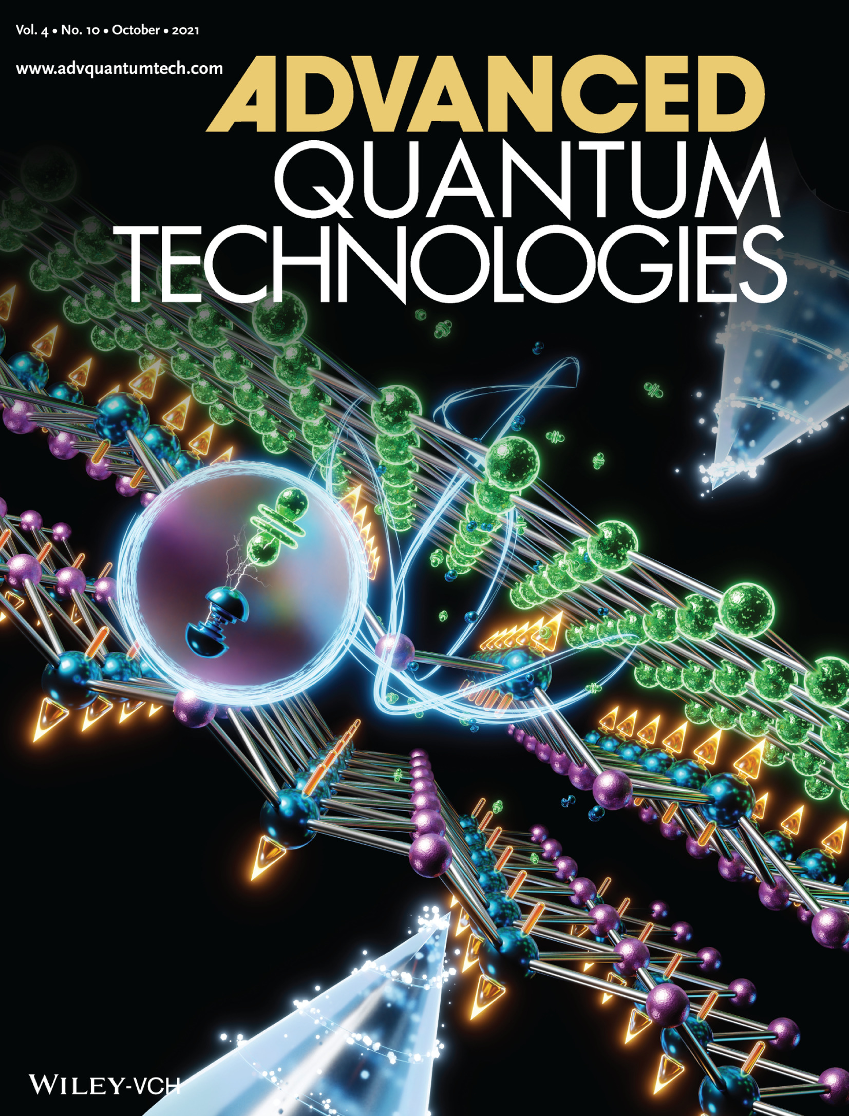
Topological materials are a promising platform for a wide range of next-generation technologies. In article number 2100063, Antonio Politano, Salvador Barraza-Lopez, Jin Hu and co-workers report a new topological material, SmSbTe, displaying a coexistence of magnetism, enhanced electronic correlations, and Dirac fermions, as illustrated in the cover image. This discovery suggests that SmSbTe represents an ideal platform for exotic quantum phenomena arising from the interplay between degrees of freedom. The manipulation of these phenomena would further pave a path for quantum material-based functional devices.
The emergence of Dirac semimetals has stimulated growing attention, owing to the considerable technological potential arising from their peculiar exotic quantum transport related to their nontrivial topological states. Especially, materials showing type-II Dirac fermions afford novel device functionalities enabled by anisotropic optical and magnetotransport properties. Nevertheless, real technological implementation has remained elusive so far. Definitely, in most Dirac semimetals, the Dirac point lies deep below the Fermi level, limiting technological exploitation. Here, it is shown that kitkaite (NiTeSe) represents an ideal platform for type-II Dirac fermiology based on spin-resolved angle-resolved photoemission spectroscopy and density functional theory. Precisely, the existence of type-II bulk Dirac fermions is discovered in NiTeSe around the Fermi level and the presence of topological surface states with strong (≈50%) spin polarization. By means of surface-science experiments in near-ambient pressure conditions, chemical inertness towards ambient gases (oxygen and water) is also demonstrated. Correspondingly, NiTeSe-based devices without encapsulation afford long-term efficiency, as demonstrated by the direct implementation of a NiTeSe-based microwave receiver with a room-temperature photocurrent of 2.8 µA at 28 GHz and more than two orders of magnitude linear dynamic range. The findings are essential to bringing to fruition type-II Dirac fermions in photonics, spintronics, and optoelectronics.
Due to their peculiar quasiparticle excitations, topological metals have high potential for applications in the fields of spintronics, catalysis, and superconductivity. Here, by combining spin- and angle-resolved photoemission spectroscopy, scanning tunneling microscopy/spectroscopy, and density functional theory, we discover surface-termination-dependent topological electronic states in the recently discovered mitrofanovite Pt3Te4. Mitrofanovite crystal is formed by alternating, van der Waals bound layers of Pt2Te2 and PtTe2. Our results demonstrate that mitrofanovite is a topological metal with termination-dependent (i) electronic band structure and (ii) spin texture. Despite their distinct electronic character, both surface terminations are characterized by electronic states exhibiting strong spin polarization with a node at the Γ point and sign reversal across the Γ point, indicating their topological nature and the possibility of realizing two distinct electronic configurations (both of them with topological features) on the surface of the same material.
We investigated the relationship between ferromagnetism and metallicity in strained La0.67Ca0.33MnO3 films grown on lattice-mismatched NdGaO3 (001) by means of spectroscopic techniques directly sensitive to the ferromagnetic state, to the band structure, and to the chemical state of the atoms. In this system, the ferromagnetic metallic (FMM) phase spatially coexists with an insulating one in most of the phase diagram. First, the observation of an almost 100% spin polarization of the photoelectrons at the Fermi level in the fundamental state provides direct evidence of the half-metallicity of the FMM phase, a result that has been previously observed through direct probing of the valence band only on unstrained, phase-homogeneous La0.67Sr0.33MnO3. Second, the spin polarization results to be correlated with the occupancy at the Fermi level for all the investigated temperature regimes. These outcomes show that the half-metallic behavior predicted by a double-exchange model persists even in phase-separated manganites. Moreover, the correlation between metallicity and ferromagnetic alignment is confirmed by X-ray magnetic circular dichroism, a more bulk-sensitive technique, allowing one to explain transport properties in terms of the conduction through aligned FMM domains.
Quantum materials are central for the development of novel functional systems that are often based on interface specific phenomena. Fabricating controlled interfaces between quantum materials requires adopting a flexible growth technique capable to synthesize different materials within a single-run deposition process with high control of structure, stoichiometry, and termination. Among the various available thin film growth technologies, pulsed laser deposition (PLD) allows controlling the growth of diverse materials at the level of single atomic layers. In PLD the atomic species are supplied through an ablation process of a stoichiometric target either in form of polycrystalline powders or of a single crystal. No carrier gases are needed in the deposition process. The ablation process is compatible with a wide range of background pressure. We present results of thin-film growth by PLD obtained by using an Nd:YAG infrared pulsed laser source operating at its first harmonics. With respect to the traditional PLD systems—based on excimer KrF UV-lasers—optimal conditions for the growth of thin films and heterostructures are reached at large target-to-substrate distance. Merits and limitations of this approach for growing oxide and non-oxide thin films are discussed. The merits of an Nd:YAG laser to grow very high-quality thin films suggest the possibility of implementing compact in-situ setups e.g. integrated with analytical instrumentation under ultra-high vacuum conditions.
The advent of topological semimetals enables the exploitation of symmetry-protected
topological phenomena and quantized transport. Here, we present homogeneous rectifiers,
converting high-frequency electromagnetic energy into direct current, based on low-energy
Dirac fermions of topological semimetal-NiTe2, with state-of-the-art efficiency already in the
first implementation. Explicitly, these devices display room-temperature photosensitivity as
high as 251 mA W−1 at 0.3 THz in an unbiased mode, with a photocurrent anisotropy ratio of
22, originating from the interplay between the spin-polarized surface and bulk states. Device
performances in terms of broadband operation, high dynamic range, as well as their high
sensitivity, validate the immense potential and unique advantages associated to the control of
nonequilibrium gapless topological states via built-in electric field, electromagnetic polar-
ization and symmetry breaking in topological semimetals. These findings pave the way for the
exploitation of topological phase of matter for high-frequency operations in polarization-
sensitive sensing, communications and imaging.
Research on ultrathin quantum materials requires full control of the growth and surface quality of the specimens in order to perform experiments on their atomic structure and electron states leading to ultimate analysis of their intrinsic properties. We report results on epitaxial FeSe thin films grown by pulsed laser deposition (PLD) on CaF2 (001) substrates as obtained by exploiting the advantages of an all-in-situ ultra-high vacuum (UHV) laboratory allowing for direct high-resolution surface analysis by scanning tunnelling microscopy (STM), synchrotron radiation X-ray photoelectron spectroscopy (XPS) and angle-resolved photoemission spectroscopy (ARPES) on fresh surfaces. FeSe PLD growth protocols were fine-tuned by optimizing target-to-substrate distance d and ablation frequency, atomically flat terraces with unit-cell step heights are obtained, overcoming the spiral morphology often observed by others. In-situ ARPES with linearly polarized horizontal and vertical radiation shows hole-like and electron-like pockets at the Γ and M points of the Fermi surface, consistent with previous observations on cleaved single crystal surfaces. The control achieved in growing quantum materials with volatile elements such as Se by in-situ PLD makes it possible to address the fine analysis of the surfaces by in-situ ARPES and XPS. The study opens wide avenues for the PLD based heterostructures as work-bench for the understanding of proximity-driven effects and for the development of prospective devices based on combinations of quantum materials.
Out-of-plane Ga2Se3 nanowires are grown by molecular beam epitaxy via Au-assisted heterovalent exchange reaction on GaAs substrates in the absence of Ga deposition. It is shown that at a suitable temperature around 560 degrees C the Audecorated GaAs substrate releases Ga atoms, which react with the incoming Se and feed the nanowire growth. The nanowire composition, crystal structure, and morphology are characterized by Raman spectroscopy and electron microscopy. The growth mechanism is investigated by X-ray photoelectron spectroscopy. We explore the growth parameter window and find an interesting effect of shortening of the nanowires after a certain maximum length. The nanowire growth is described within a diffusion transport model, which explains the nonmonotonic behavior of the nanowire length versus the growth parameters. Nanowire shortening is explained by the blocking of Ga supply from the GaAs substrate by thick, in-plane worm-like Ga2Se3 structures, which grow concomitantly with the nanowires, followed by backward diffusion of Ga atoms from the nanowires down to the substrate surface.
Chiral crystal YbNi3Ga9 is known as an intermediate valence compound in which a strong hybridization between the 4f orbitals and the conduction band is present. The Co-substitution to YbNi3Ga9 works as a hole doping that reduces the Kondo temperature and enhances the effective mass of itinerant charge carriers. Using angle-resolved photoelectron spectroscopy, the complex band structure of Yb(Ni1−xCox)3Ga9 (x=0,0.1) is revealed. A Yb2+ 4f7/2 band and evidences of hybridization to valence bands are found near the Fermi level. Both YbNi3Ga9 and the Co-substituted compound exhibit double hexagonal Fermi surfaces centered at the Γ¯-point, surrounded by a large snowflake-like surface, and a triangular electron-like surface along the Γ¯M¯ direction. By changing the incident photon energy, the band dispersion along the c-axis and the barrel-shaped Fermi surface is observed.
We predict NiTe2 to be a type-II Dirac semimetal based on ab initio calculations and explore its bulk and spin-polarized surface states using spin- and angle-resolved photoemission spectroscopy (spin-ARPES). Our results show that, unlike PtTe2, PtSe2, and PdTe2, the Dirac node in NiTe2 is located in close vicinity to the Fermi energy. Additionally, NiTe2 also hosts a pair of band inversions below the Fermi level along the Γ−A high-symmetry direction, with one of them leading to a Dirac cone in the surface states. The bulk Dirac nodes and the ladder of band inversions in NiTe2 support unique topological surface states with chiral spin texture over a wide range of energies. Our work paves the way for the exploitation of the low-energy type-II Dirac fermions in NiTe2 in the fields of spintronics, infrared plasmonics, and ultrafast optoelectronics.
The layered van der Waals antiferromagnet MnBi2Te4 has been predicted to combine the band ordering of archetypical topological insulators such as Bi2Te3 with the magnetism of Mn, making this material a viable candidate for the realization of various magnetic topological states. We have systematically investigated the surface electronic structure of MnBi2Te4(0001) single crystals by use of spin- and angle-resolved photoelectron spectroscopy experiments. In line with theoretical predictions, the results reveal a surface state in the bulk band gap and they provide evidence for the influence of exchange interaction and spin-orbit coupling on the surface electronic structure.