FACILITY AT NFFA-TRIESTE
An UHV STM/STS instrument capabe of atomic resolution but limited to room temperature. The samples can be directly uploaded and/or exchanged with the Surface and Nano Science Lab and the whole suite of APE-NFFA chambers.
The STM/STS has been built at ETH-Zuerich Laboratorium fuer Festkoerperphysik, and is controlled by Dulcinea Control Unit (Nanotec Electronica S.L.) units and WSxM (WSxM solutions) software. The operation of the STM/STS is compatible with the simultaneous operation of the other end-stations.
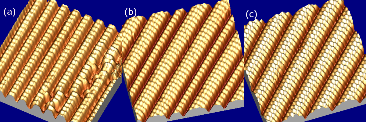
STM topographic images for 2 different phases of Bi (10nm x 10nm). (a)4x1, (b)mixture 4x1 and 6x1, (c)6x1
IMAGE PREVIEW
STM topographic images for 2 different phases of Bi (10nm x 10nm). (a)4x1, (b)mixture 4x1 and 6x1, (c)6x1
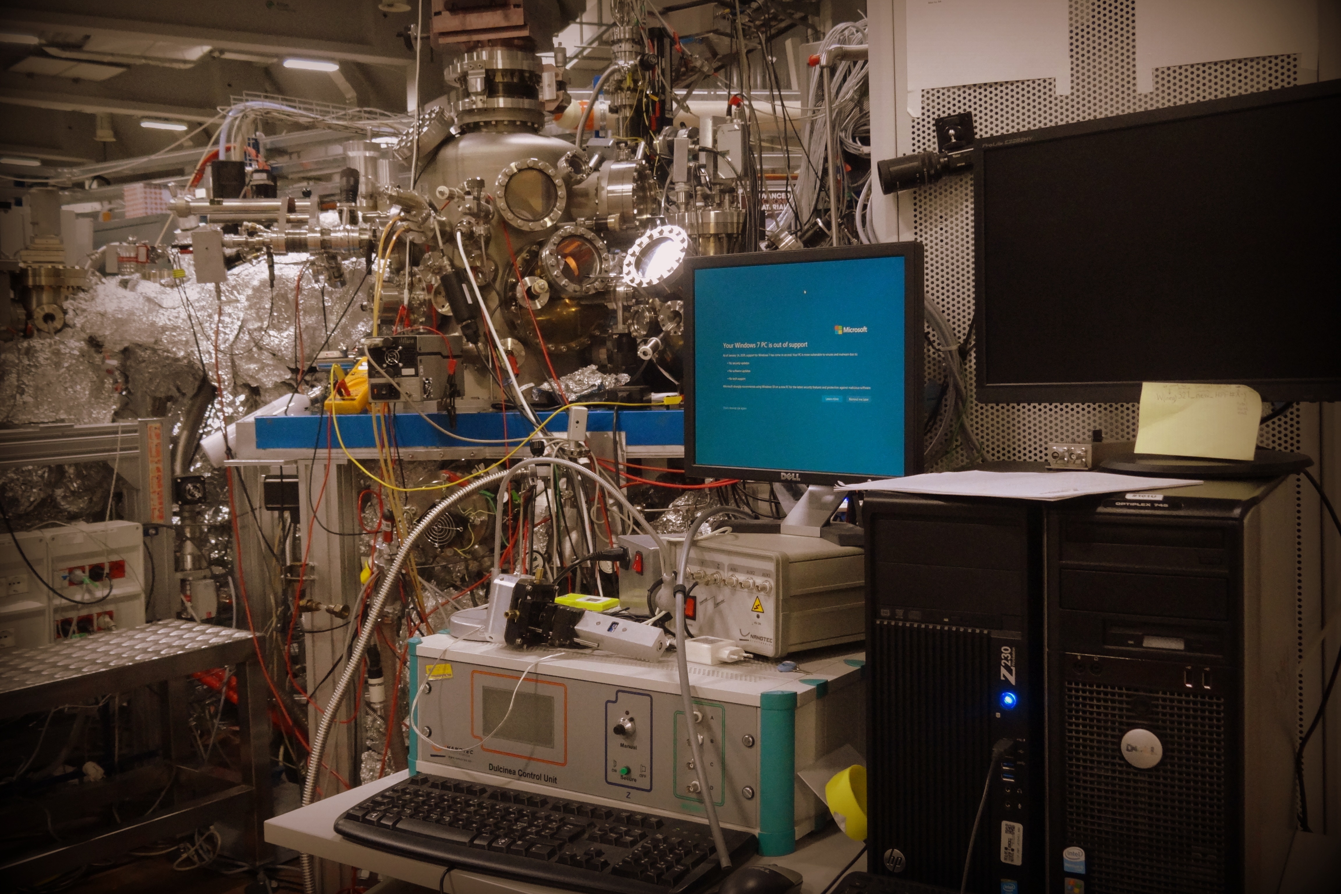
IMAGE PREVIEW
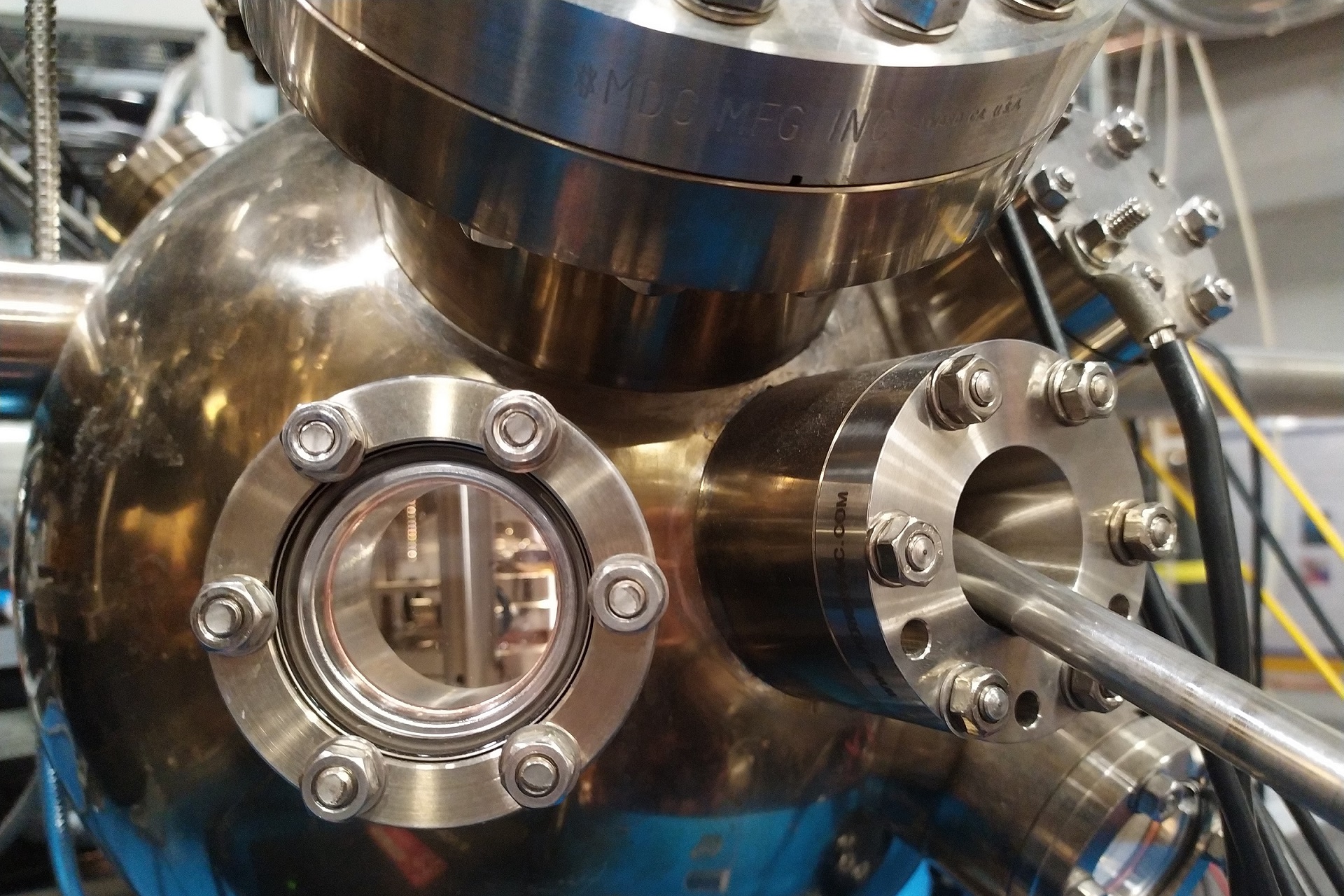
IMAGE PREVIEW
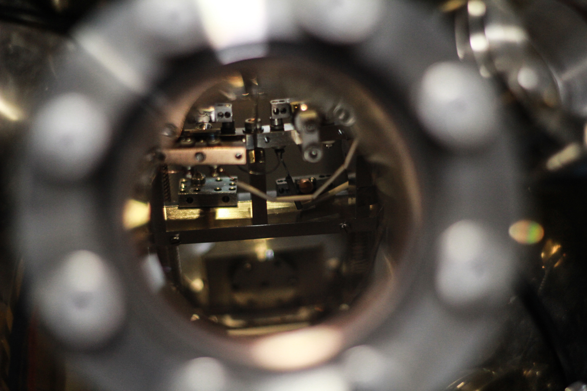
IMAGE PREVIEW
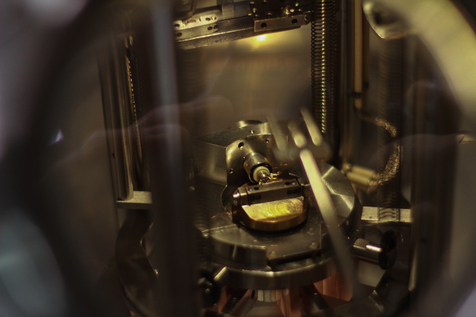
IMAGE PREVIEW
